The usual progression for making printed circuits is (very roughly) you design the circuit, prototype it on a breadboard, design your PCB, and iterate on your PCB design.
Impatient hands
I’m a bit too impatient to wait for the PCB part. Also, I learn better having things in my hands. Iterating at the PCB design level, where you need to wait days, if not weeks, for your PCB board to come back, isn’t ideal for my impatient ways.
What I noticed is that after prototyping the circuit, I like to lay it out on cardboard. Doing this gives me a feel for scale, arrangement, and process.
Of course, for now, I’m doing it with through-hole components, though I am debating doing it with with surface mount devices.
One thing at a time.
As for ‘one thing at a time‘, cardboard prototyping also fits in well with how I set myself to learn. I get to focus on one thing at a time. Be it, design, or new arrangement of parts, or a new circuit type. I think before you hit the PCB design, the level of learning to get there needs a few more steps than usual.
Some recent cardboard projects
I mentioned what I’ve been doing to learn #badgelife concepts. The whole process of printing and pasting onto cardboard was helpful in giving me an understanding of scale and packing of components.
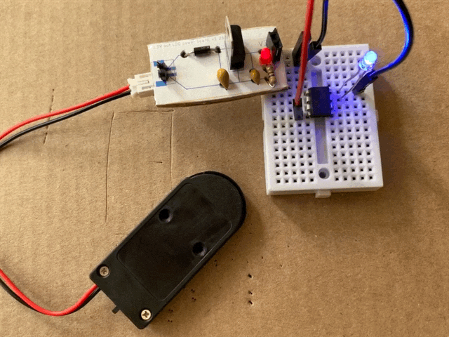
Yesterday, I spent the day building a 3.3V power regulator on cardboard (see GIF above of it in action). I had read schematics on how to make one. Bought components to try it out on a breadboard. And then put it on a schematic to print and guide building of the circuit on a piece of cardboard.
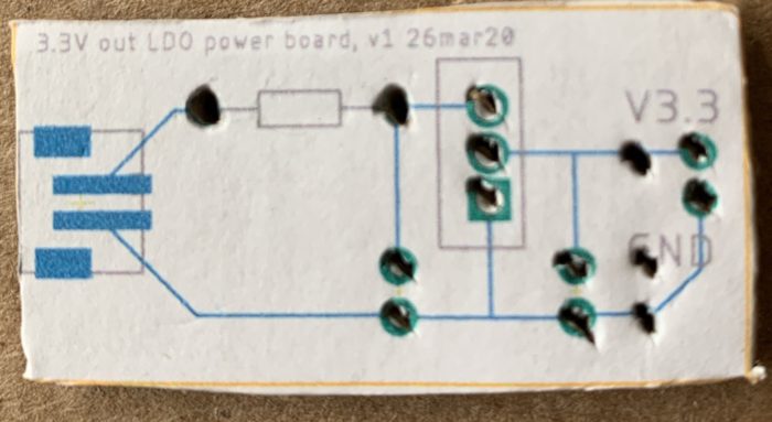
Top, ready for components [note extra unmarked holes for LED and resistor] 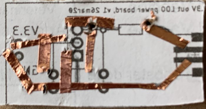
Initial copper circuit laid out [note that the bottom is a bit off register from the top, so will need to fix next time] 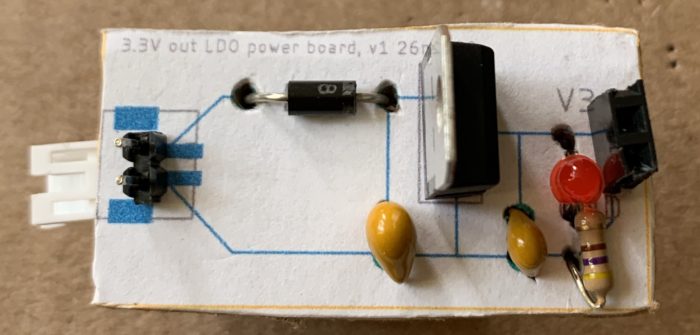
Top, with components in 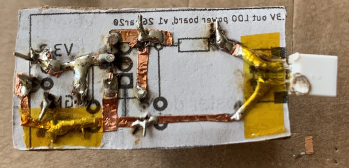
Messy soldering underneath, but works Testing board. Power light ON, (old) batteries giving about 4.something V, powering ATtiny85 with a blink program. Works!
Interestingly, by futzing with it in my hand, I saw an opportunity for an on-the-fly change, adding a resistor and a diode to indicate power was on.
And the process reinforced some insights I gained while doing other similar cardboard-based circuits around soldering on the copper tape, handling and laying down copper tape, bridging the components and the coper circuit, and, of course, scale.
Surface mount, anyone?
From the cardboard proto of that owl badge I’ve been working on, I went and made a PCB. The PCB will be for through-hole components. The exercise was really to see if I could make a custom outline, silk, resist, and copper pours (fun stuff). I didn’t want to also have to learn other SMD-related issues.
Also, I know when the board comes in I’ll learn a bit about handling the boards, soldering many boards, and how might it hang from a lanyard – things I knew best learned with a first run of PCBs.
The next step is to convert the badge to mostly SMD, mostly to keep the front pristine, but also to learn how to search and buy surface mount components (soooo many). But I’m wondering if I should do a round of cardboard protos, first. SMD components will allow me to shrink the board somewhat (sand save money). Might want to try that out on cardboard rather than via PCB iterations.
Let’s see. In any case, I will report back.
And then there’s brass
As a parting thought, I read up on free-form circuits built from brass rods. Check out these guys. Lovely sculptures.
Haha. One more process to learn and tinker with.
What about you?
What materials are you working with outside the usual? Wood? Paper? Fabric?
Let me know Send me links of your work!